240-Pin Unbuffered DIMM DDR3 SDRAM
http://www.supertalent.com/oem Products and Specifications discussed herein are subject to change without notice
2 © 2006 Super Talent Tech., Corporation.
1.0 Feature
• JEDEC standard 1.5V ± 0.075V Power Supply
•
VDDQ = 1.5V ± 0.075V
• Programmable CAS latencies 6,7,8,9,10,11,13
•
Programmable Additive Latency(Posted CAS) : 0, CL - 2, or CL - 1 clock
•
Programmable CAS Write Latency(CWL) = 5 (DDR3-800), 6 (DDR3-1066), 7 (DDR3-1333), 8 (DDR3-1600) and 9 (DDR3-1866)
•
400MHz fCK for 800Mb/sec/pin, 533MHz fCK for 1066Mb/sec/pin, 667MHz fCK for 1333Mb/sec/pin, 800MHz fCK for
1600Mb/sec/pin,
900MHz fCK for 1866Mb/sec/pin
• Bi-directional Differential Data Strobe
•
Burst Length: 8 (Interleave without any limit, sequential with starting address “000” only), 4 with tCCD = 4 which does not allow seamless
read or write [either On the fly using A12 or MRS]
• On-Die termination using ODT pin
• 8 independent internal bank
•
Asynchronous Reset
• Average Refresh Period 7.8us at lower than a TCASE 85°C, 3.9us at 85°C < TCASE < 95 °C
• Serial presence detect with EEPROM
• DIMM Dimension (Nominal) 30.00 mm high, 133.35 mm wide
• Based on JEDEC standard reference Raw Cards Lay out.
• RoHS compliant
• Gold plated contacts
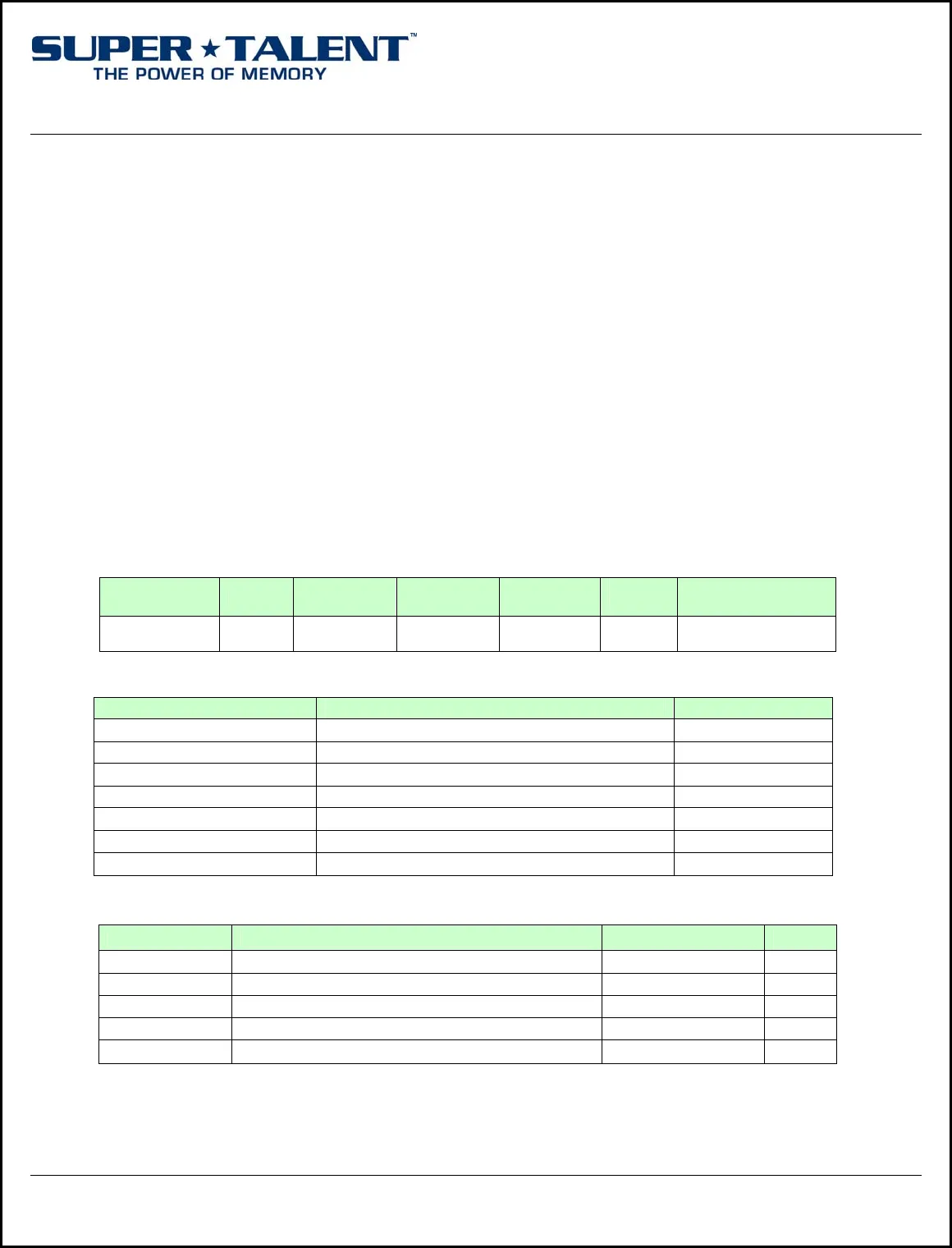
2.0 Ordering Information
Part number Density
Module
Organization
Component
composition
Component
PKG
Module
Rank
Description
W1333UB4GV 4GB 512Mx64 256Mx8*16 TFBGA 2
4GB 2Rx8 PC3-
10600U
3.0 Key Timing Parameters
DDR3-1333 Unit
CL-tRCD-tRP
9-9-9
tCK
CAS Latency
9
tCK
tCK(min)
1.5
ns
tRCD(min)
13.5
ns
tRP(min)
13.5
ns
tRAS(min)
36
ns
tRC(min)
49.5
ns
4.0 Absolute Maximum DC Rating
Symbol Parameter Rating Units
V
in ,
Vout Voltage on any pin relative to V
SS
-0.4 ~ 1.975 V
V
DD
Voltage on V
DD
& V
DDQ
supply relative to V
ss
-0.4 ~ 1.975 V
V
DDQ
Short circuit current -0.4 ~ 1.975 V
V
DDL
Power dissipation -0.4 ~ 1.975 V
T
STG
Storage Temperature -55 ~ + 100 °C