AP6503A
Document number: DS36000 Rev. 2 - 2
4 of 15
www.diodes.com
December 2012
© Diodes Incorporated
NEW PRODUCT
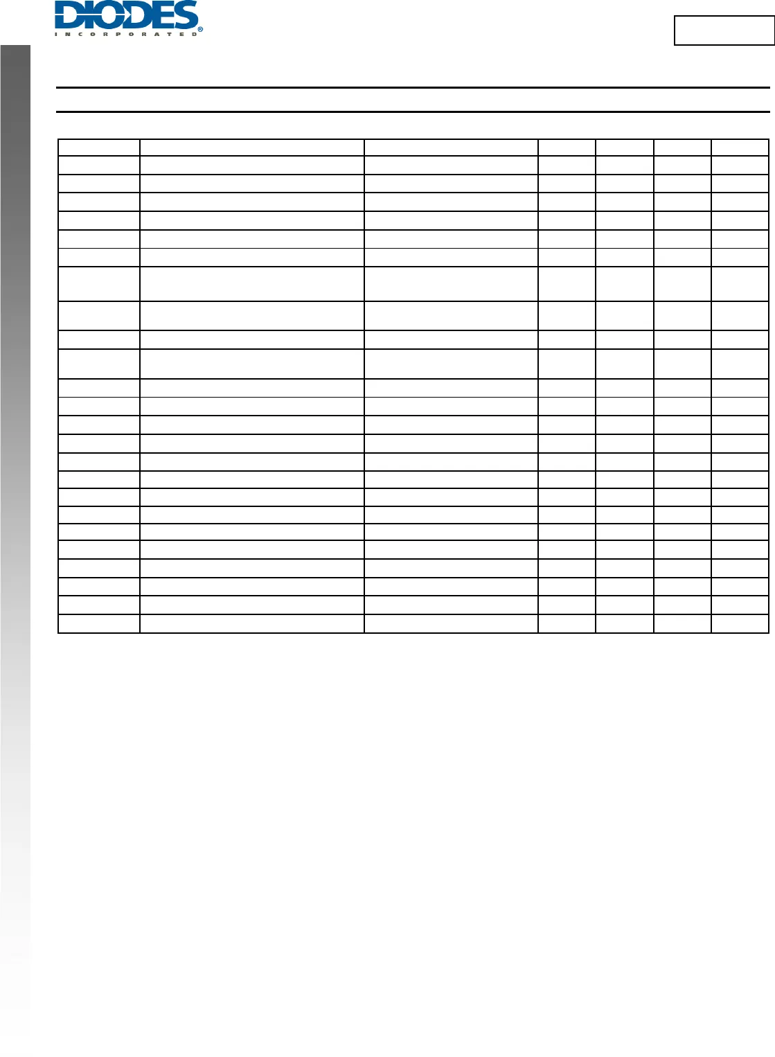
P6503A
Electrical Characteristics (V
IN
= 12V, @T
A
= +25°C, unless otherwise specified.)
Symbol Parameter Test Conditions Min Typ Max Unit
I
IN
Shutdown Supply Current
V
EN
= 0V
— 0.3 3.0 µA
I
IN
Supply Current (Quiescent)
V
EN
= 2.0V, V
FB
= 1.0V
— 0.6 1.5 mA
R
DS(ON)1
High-Side Switch On-Resistance (Note 8) — 100 — m
R
DS(ON)2
Low-Side Switch On-Resistance (Note 8) — 100 — m
I
LIMIT
HS Current Limit Minimum duty cycle — 5.5 — A
I
LIMIT
LS Current Limit From Drain to Source — 0.9 — A
High-Side Switch Leakage Current
V
EN
= 0V, V
SW
= 0V,
V
SW
=12V
— 0 10 A
AVEA
Error Amplifier Voltage Gain
(Note 8)
— 800 — V/V
GEA Error Amplifier Transconductance
I
C
= ±10µA
— 1000 — µA/V
GCS
COMP to Current Sense
Transconductance
— 2.8 — A/V
F
SW
Oscillator Frequency
V
FB
= 0.75V
210 240 260 kHz
F
FB
Fold-back Frequency
V
FB
= 0V
— 0.30 —
f
SW
D
MAX
Maximum Duty Cycle
V
FB
= 800mV
— 90 — %
T
ON
Minimum On Time — 130 — ns
V
FB
Feedback Voltage
T
A
= -40°C to +85°C
900 925 950 mV
Feedback Overvoltage Threshold — 1.1 — V
V
EN_Rising
EN Rising Threshold 0.7 0.8 0.9 V
EN Lockout Threshold Voltage 2.2 2.5 2.7 V
EN Lockout Hysteresis 220 mV
INUV
VTH
V
IN
Under Voltage Threshold Rising
3.80 4.05 4.40 V
INUV
HYS
V
IN
Under Voltage Threshold Hysteresis
— 250 — mV
Soft-Start Current
V
SS
= 0V
— 6 — A
Soft-Start Period
C
SS
= 0.1µF
— 15 — ms
T
SD
Thermal Shutdown (Note 8) — 160 — °C
Note: 8. Guaranteed by design