AP5101
1.5A Step-Down Converter with 1.4MHz Switching
Frequency
AP5101
Document number: DS32258 Rev. 1 - 2
3 of 15
www.diodes.com
July 2010
© Diodes Incorporated
NEW PRODUCT
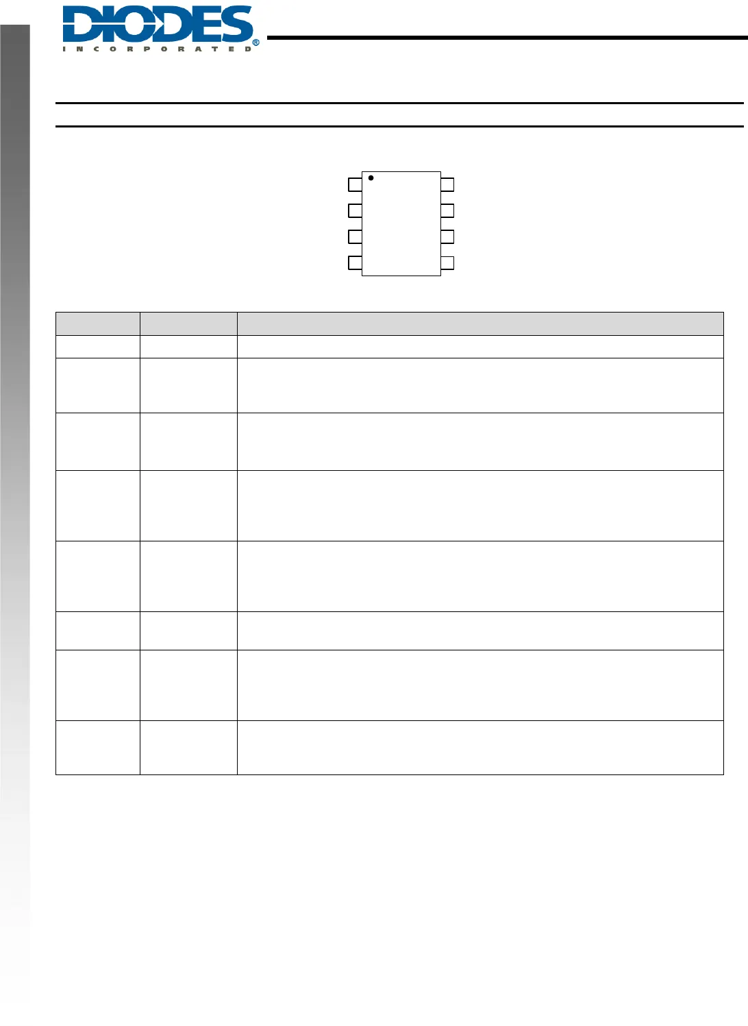
Pin Descriptions
SO-8
( Top View )
1
2
3
4
8
7
6
5
GND
BST
FB
COMP
SW
GND
EN
IN
Pin Name Pin Number Descriptions
SW 1 Switch Output. This is the reference for the floating top gate driver.
IN
2
Supply Voltage. The AP5101 operates from a +4.75V to +22V unregulated
input. A decoupling capacitor C1 is required to prevent large voltage spikes
from appearing at the input. Place this capacitor near the IC.
EN
3
On/Off Control Input. Do not leave this pin floating. To turn the device ON, pull
EN above 1.2V and to turn it off pull below 0.4V.
If enable/disable is not used, connect a 100kΩ resistor between EN to V
IN
.
GND
4
Ground. This pin is the voltage reference for the regulated output voltage. For
this reason care must be taken in its layout. This node should be placed
outside of the D1 to C1 ground path to prevent switching current spikes from
inducing voltage noise into the part.
FB
5
Feedback. To set the output voltage, connect this pin to the output resistor
divider or directly to V
OUT
. To prevent current limit run away during a current
limit condition, the frequency foldback comparator lowers the oscillator
frequency when the FB voltage is below 400mV.
COMP
6
Compensation. COMP is used to compensate the regulation control loop.
Connect a series RC network from COMP to GND.
BST
7
Bootstrap. To form a boost circuit, a capacitor is connected between SW and
BST pins to form a floating supply across the power switch driver. This
capacitor is needed to drive the power switch’s gate above the supply voltage.
Typical values for C
BST
range from 0.1uF to 1uF.
GND
8
Ground. This pin is the voltage reference for the regulated output voltage. All
control circuits are referenced to this pin. For this reason care must be taken in
its layout.