Advantech SOM-Express Design Guide
Chapter 3 Pin Assignments 31
Chapter 3 Pin Assignments
This chapter describes pin assignments and IO characteristics for the 440 pin SOM-
Express. It includes four parts (A, B, C, D). There are five types of pin assignments
for COM-Express. We chose type-2 pin assignments on the SOM-Express. Please
refer to the COM-Express specifications to get more information.
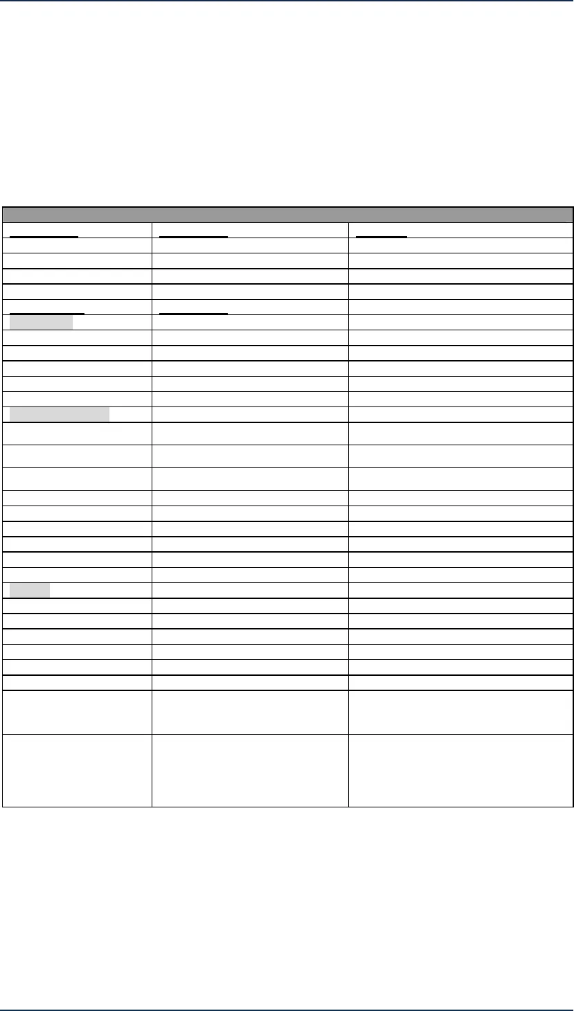
Figure 3-1 SOM-Express Diagram
Table 3.1 Conventions and Terminology
Convention Description Example
‘#’ Active-Low Signals WAKE0#
‘+’ and ‘-’ Differential Pairs SATA0_TX+, SATA0_TX-
Terminology Description
Pin Types:
I Input
O Output
IO Bi-Directional
OD Open Drain
Power Pin Types
VCC2.5
+2.5 V ± 5% Volts
VCC3
+3.3 V ± 5% Volts
VSB3
+3.3 V ± 5% Standby Power
VCC3/5 +3.3 V and +5 V tolerance
GND System Ground
PWR Power Supply
AC on AC coupled on module
AC off AC coupled off module
Others
I/F Interface
MISC Miscellaneous Interface
NC Not Connected. Reserved.
P Power Plane
RSVD Reserved pin
*1 GND min, 3.3 V max
REF Reference voltage output. May
be sourced from a module
power plane.
PDS Pull-down strap. A module
output pin that is either tied to
GND or is not connected.
Used to signal module
capabilities to the Carrier Board.
Notes:
1. PWR*: The power to this pin is supplied from the carrier board connected to the
power supply.
2.
Please refer to Chapter 5 for detailed descriptions.